Key Takeaways: This post explores the transformative role of laser annealing technology in silicon carbide (SiC) wafer processing. We delve into technical concepts, practical applications, and learning opportunities that can enhance your career in semiconductor manufacturing. By the end, you’ll have actionable insights and a roadmap for skill development in this rapidly evolving field.
Introduction
As the demand for silicon carbide (SiC) semiconductor devices surges, particularly in the electric vehicle and renewable energy sectors, mastering the techniques and technologies behind their fabrication becomes increasingly crucial. Laser annealing technology stands at the forefront of this transformation, providing precise control over the activation of dopants, reduction of defects, and optimization of crystalline structures. This blog post aims to equip developers, IT professionals, and tech learners with a comprehensive understanding of laser annealing technology, its applications, and the educational paths leading to mastery in this field.
Technical Background and Context
Laser annealing technology utilizes high-power laser sources to deliver controlled thermal energy to silicon carbide wafers. This advanced technique is instrumental in achieving:
📚 Recommended Digital Learning Resources
Take your skills to the next level with these curated digital products:
Academic Calculators Bundle: GPA, Scientific, Fraction & More
Academic Calculators Bundle: GPA, Scientific, Fraction & More
ACT Test (American College Testing) Prep Flashcards Bundle: Vocabulary, Math, Grammar, and Science
ACT Test (American College Testing) Prep Flashcards Bundle: Vocabulary, Math, Grammar, and Science
📊 Key Learning Points Infographic
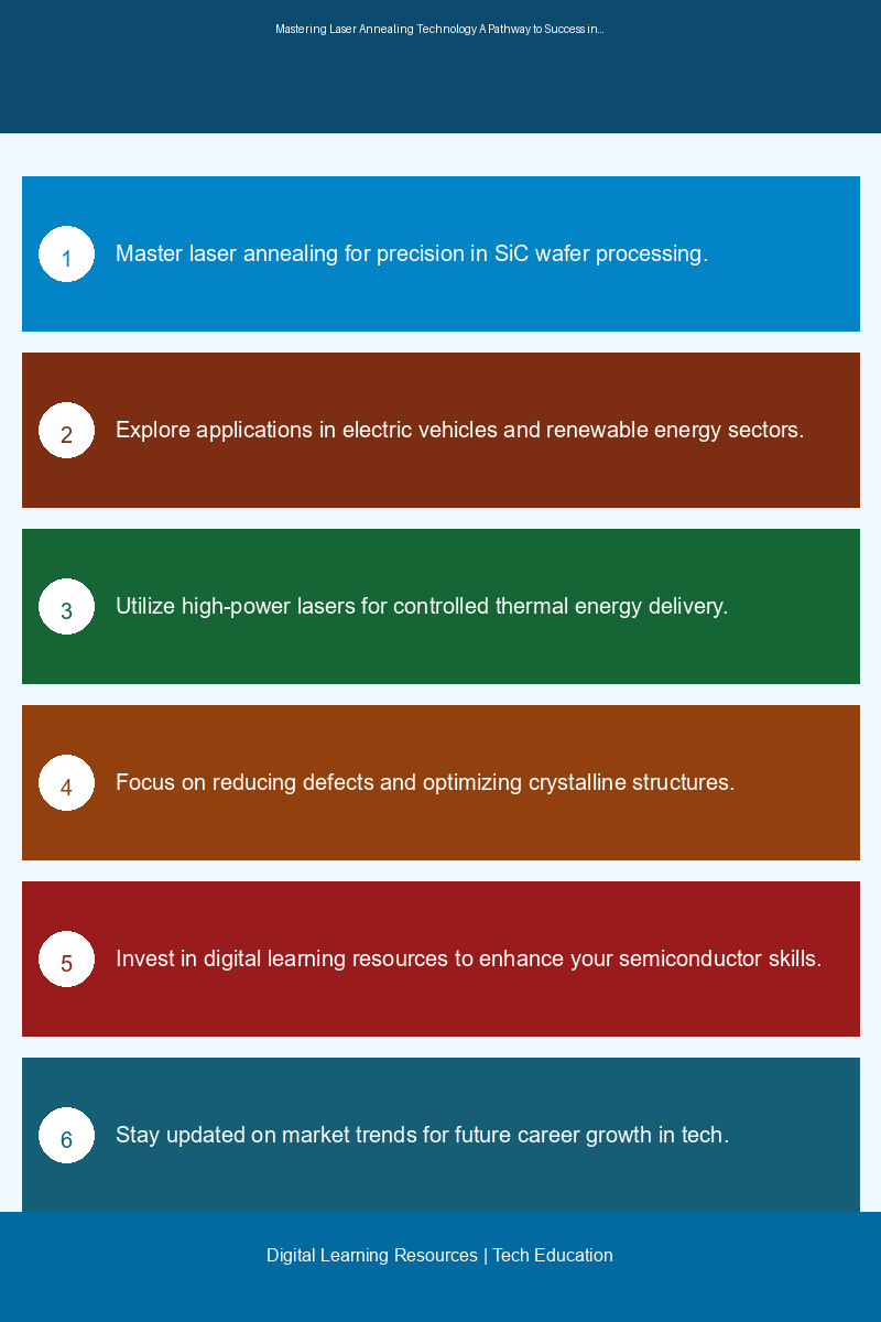
Visual summary of key concepts and actionable insights
Leonardo.Ai API Mastery: Python Automation Guide (PDF + Code + HTML
Leonardo.Ai API Mastery: Python Automation Guide (PDF + Code + HTML
100 Python Projects eBook: Learn Coding (PDF Download)
100 Python Projects eBook: Learn Coding (PDF Download)
HSPT Vocabulary Flashcards: 1300+ Printable Study Cards + ANKI (PDF)
HSPT Vocabulary Flashcards: 1300+ Printable Study Cards + ANKI (PDF)
- Dopant Activation: Enhancing the electrical properties of SiC by activating dopants effectively.
- Defect Reduction: Minimizing structural defects that can hinder device performance.
- Crystalline Structure Optimization: Improving the overall quality of the crystal lattice for better electronic characteristics.
Critical to the laser annealing process are precision temperature control systems that enable rapid heating and cooling cycles. Multi-zone temperature monitoring allows for tailored thermal profiles across the wafer, while advanced beam shaping technology ensures that the laser energy is applied uniformly. Sophisticated process control algorithms facilitate the optimization of annealing parameters, resulting in enhanced yield and reliability.
Practical Applications and Use Cases
The applications of laser annealing technology extend across various sectors, particularly in semiconductor manufacturing:
- Electric Vehicles: SiC devices are crucial for power electronics in EVs, where efficiency and performance are paramount.
- Renewable Energy: SiC components are employed in solar inverters and power management systems, aiding the transition to sustainable energy solutions.
- Telecommunications: High-frequency applications benefit from the improved thermal and electrical characteristics of SiC semiconductors.
By integrating laser annealing into the manufacturing process, companies can significantly enhance the performance and durability of their semiconductor devices, aligning with industry demands for efficiency and sustainability.
Learning Path Recommendations
To thrive in the laser annealing and semiconductor manufacturing landscape, consider the following educational opportunities:
- Courses on Semiconductor Manufacturing Processes: Gain a foundational understanding of the various steps involved in semiconductor production.
- Training in Laser Technology: Explore how lasers are utilized in materials processing, focusing on the principles of laser annealing.
- Programs on Wide Bandgap Semiconductor Materials: Learn about the properties and applications of materials like SiC and GaN.
- Workshops on Process Control: Participate in hands-on training focused on optimizing manufacturing processes and enhancing yield.
These learning paths will provide you with valuable skills that are directly applicable to the semiconductor industry, enhancing your employability and career prospects.
Industry Impact and Career Implications
The semiconductor industry is undergoing significant transformation, driven by technological advancements and changing market demands. The growth of the 4-inch SiC laser annealing equipment market is projected to increase by 290.8% from 2025 to 2035. This growth signifies a burgeoning need for skilled professionals who can leverage these technologies in manufacturing environments.
As electric vehicle adoption accelerates and renewable energy infrastructures expand, the demand for SiC devices will continue to rise. Professionals with expertise in laser annealing, semiconductor processing, and advanced manufacturing technologies will be well-positioned for career advancement in this dynamic field.
Implementation Tips and Best Practices
To effectively implement laser annealing technology in a manufacturing context, consider the following best practices:
- Invest in High-Quality Equipment: Utilize advanced 4-inch SiC laser annealing equipment with various laser configurations to ensure optimal performance.
- Integrate Automation Systems: Streamline processes with automation, reducing manual errors and increasing throughput.
- Employ Data Analytics Tools: Utilize data analytics to monitor yield and process reliability, making informed adjustments to optimize performance.
- Focus on Continuous Improvement: Regularly assess and refine annealing parameters based on real-time monitoring feedback to enhance process efficiency.
Future Trends and Skill Requirements
As the semiconductor industry evolves, several trends are likely to shape the future of laser annealing technology:
- Increased Focus on Sustainability: The industry will continue to prioritize energy-efficient and environmentally friendly manufacturing practices.
- Advancements in Process Control: Enhanced algorithms and real-time monitoring systems will drive improvements in process optimization.
- Growing Importance of Predictive Maintenance: Predictive maintenance capabilities will become essential for reducing downtime and ensuring operational efficiency.
To stay competitive, aspiring professionals should focus on acquiring skills in semiconductor device fabrication, laser technology, and process optimization. Certifications in advanced manufacturing technologies will also enhance your qualifications and marketability.
Conclusion with Actionable Next Steps
Laser annealing technology is revolutionizing the semiconductor manufacturing landscape, offering numerous opportunities for professionals willing to invest in their education and skill development. To embark on your journey:
- Identify relevant courses and workshops that align with your career goals.
- Engage with industry professionals through networking events and online forums.
- Stay updated on industry trends and emerging technologies to remain competitive.
- Consider pursuing certifications in semiconductor manufacturing and laser technology to validate your expertise.
By taking these actionable steps, you can position yourself for success in the rapidly evolving field of semiconductor manufacturing and harness the full potential of laser annealing technology.
Disclaimer: The information in this article has been gathered from various reputed sources in the public domain. While we strive for accuracy, readers are advised to verify information independently and consult with professionals for specific technical implementations.
Ready to advance your tech career? Explore our digital learning resources including programming guides, certification prep materials, and productivity tools designed by industry experts.